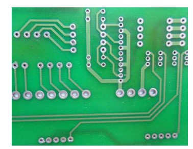
Single Sided PCB
Cost-effective and reliable single-sided PCBs ideal for simple electronic devices.
Capabilities
- Material: FR4, 370HR, Rogers...etc.
- Board Thickness: 0.8 to 3.2 mm
- Copper Weight: 35 to 105 Micron
- Surface Finish: Roller Tin, HAL, LF-HAL, ENIG, Silver...etc.
- Min Hole Size : 0.3mm*
- Min Annular Ring : 0.1 mm
- Min Track / Space : 0.1 mm
- Solder Mask Colour : Green, Blue, Red, Black, White
- Silk Screen Colour : White, Black
Fabrication Process
Data Preparation & Verification
Imaging & Photoresist Application
Etching
Surface Finish
Inspection & Testing
Double Sided PCB (PTH)
High quality double-sided PCBs with plated through holes for complex, dense circuits.
Capabilities
- Material: FR4, 370HR, Rogers...etc.
- Board Thickness: 0.8 to 3.2 mm
- Copper Weight: 35 to 105 Micron
- Surface Finish: HAL, LF-HAL, ENIG, Silver...etc.
- Min Hole Size : 0.2 mm*
- Min Annular Ring: 0.1 mm
- Min Track/Space: 0.1 mm
- Solder Mask Colour : Green, Blue, Red, Black, White
- Silk Screen Colour : White, Black
Fabrication Process
File Verification
Inner Layer Imaging & Etching
Drilling & Plating
Surface Finishing
Quality Inspection
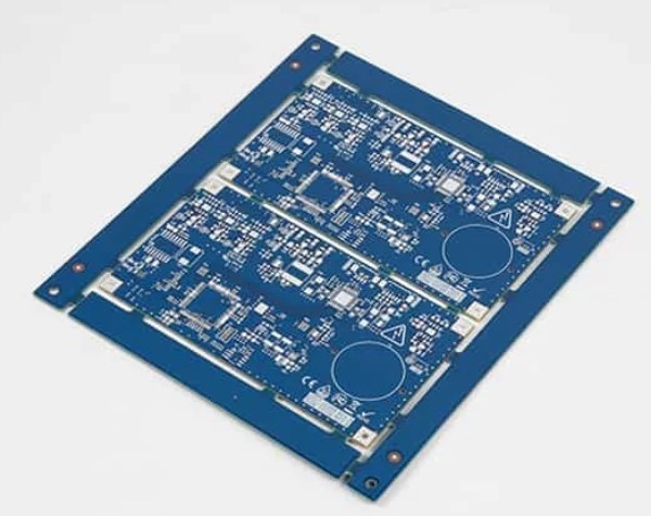
Multi Layer PCB
Multilayer PCBs offering high-density routing, thermal management, and high-speed performance.
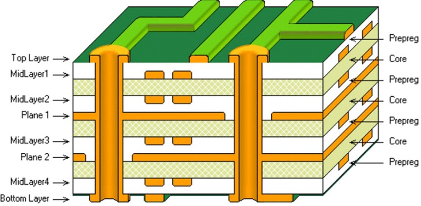
Capabilities
- Material: FR4, 370HR, Rogers...etc.
- Board Thickness: 0.6 to 4.5 mm
- Copper Weight: 18 to 105 Micron
- Surface Finish: HAL, LF-HAL, ENIG, Silver...etc.
- Min Hole Size : 0.1 mm*
- Min Annular Ring: 0.1 mm
- Min Track/Space: 0.1 mm
- Solder Mask Colour : Green, Blue, Red, Black, White
- Silk Screen Colour : White, Black
Fabrication Process
Design File Preparation & Data Preparation and Verification
Inner Layer Imaging & Etching
Layer Alignment & Lamination
Drilling & Plating
Finishing & Solder Mask Application
Inspection, Testing & Quality Control
Flexible PCB
Flexible circuits built for dynamic forms and compact designs with excellent durability.
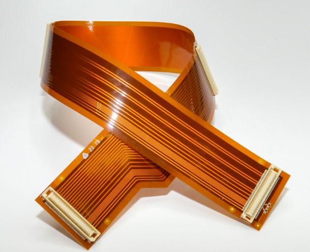
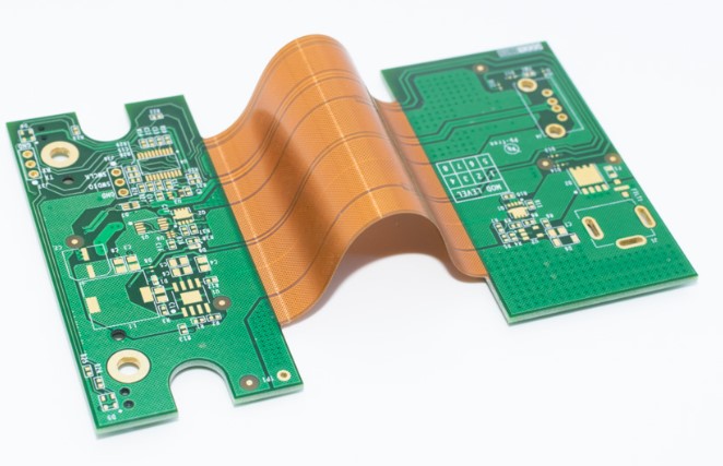
Capabilities
- Optimized bend radius and flex cycles
- Single, double, and multilayer flex options
- Polyimide and polyester substrates
- Adhesive and adhesive-less constructions
Fabrication Steps
File & Material Preparation
Imaging & Etching
Lamination & Curing
Drilling & Plating
Surface Treatment & Solder Mask
Testing & Inspection
HDI PCB
High-Density Interconnect PCBs with ultra-fine lines and microvias for miniaturization.
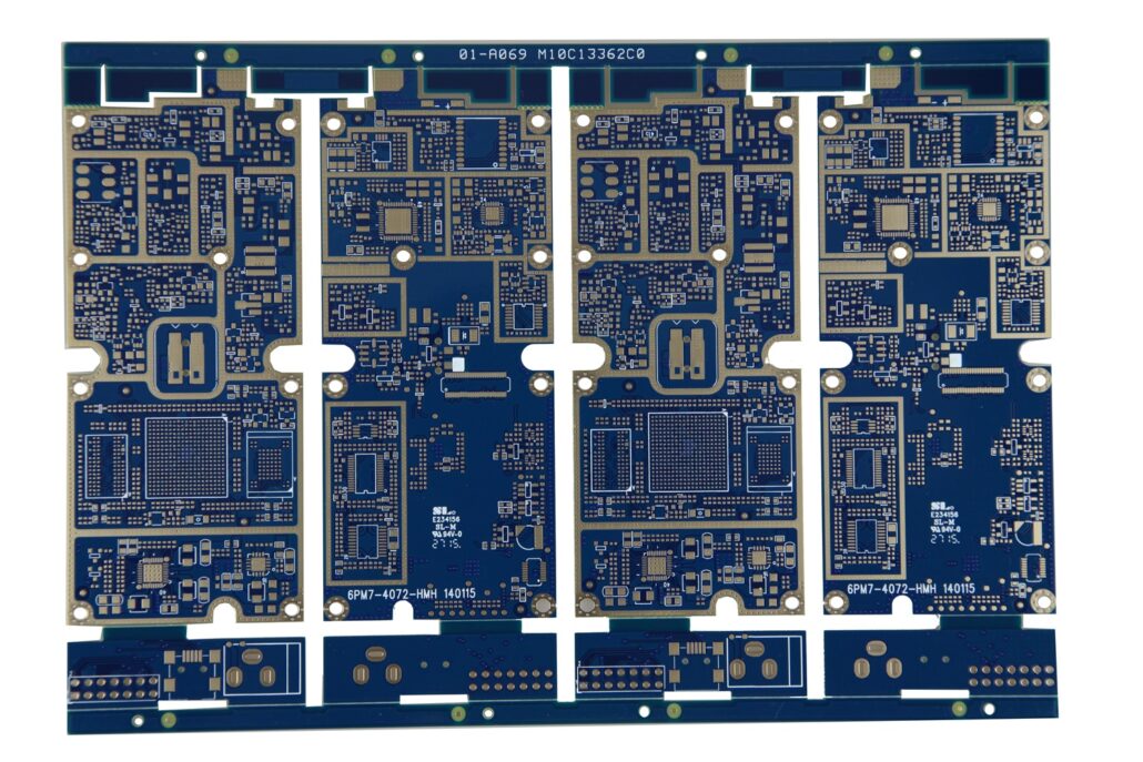
Capabilities
- Microvia and blind/buried via technology
- Laser drilling and selective plating
- Fine line and space down to 50 microns
- High reliability and performance
Fabrication Process
Data Validation & CAM Planning
Laser Imaging & Inner Layer Formation
Multi-layer Lamination
Microvia Drilling & Plating
Surface Finish & Final Processing
Final Inspection & Testing
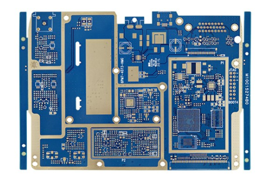
User Case
Use Case: High-Speed Data Acquisition Board
Industry: Test & Measurement / Industrial Electronics
Objective: Fabricate a precision 6-layer PCB for a high-speed data acquisition system with tight impedance control and low signal loss.